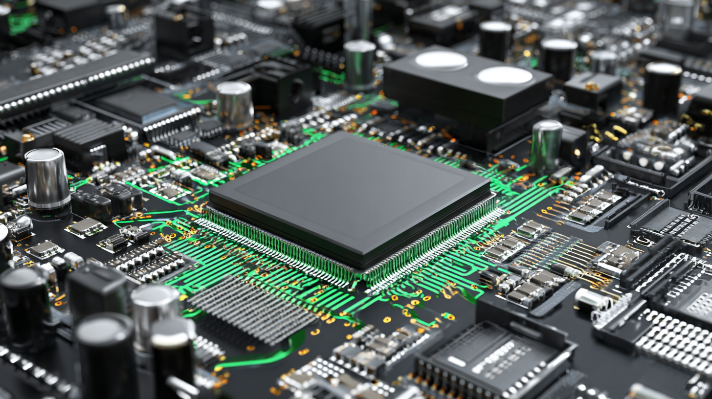
How to Optimize Your PCB Electronics Design for Maximum Efficiency
In the rapidly evolving world of electronics, the efficiency of your designs can significantly impact performance, cost, and sustainability. Optimizing your PCB electronics design is essential for achieving these goals, as it influences everything from signal integrity to thermal management. As devices become more compact and require greater functionality, understanding the principles of PCB electronics becomes increasingly important.
This guide will delve into effective strategies for maximizing efficiency in your designs, from selecting the right materials and components to implementing advanced layout techniques. By following these best practices, you can ensure that your PCB electronics not only meet industry standards but also excel in performance, durability, and cost-effectiveness.
Join us as we explore how to fine-tune your designs and enhance the overall capability of your electronic projects.
Understanding the Basics of PCB Design for Optimal Performance
When it comes to optimizing PCB design for maximum efficiency, a fundamental understanding of the basics is crucial. According to a 2022 report by IPC, the global electronics manufacturing industry is projected to reach $1 trillion by 2025, highlighting the significant role that well-designed PCBs play in ensuring product reliability and performance. Key design principles include minimizing trace length, managing signal integrity, and proper grounding techniques. Ensuring that power delivery networks are efficient can reduce the risk of electromagnetic interference (EMI), a major concern in high-speed applications.
Another critical aspect is thermal management. The NEMA 2021 survey indicates that nearly 70% of PCB failures can be attributed to thermal issues. Therefore, integrating features such as thermal vias and copper pours can enhance heat dissipation and prolong the lifespan of components. Furthermore, adopting design methodologies like Design for Manufacturability (DFM) not only streamlines the production process but also reduces costs significantly, as noted in a 2023 market analysis by TechNavio, which found that efficient PCB designs can lead to cost savings of up to 25%. Emphasizing these foundational elements in PCB design will ultimately lead to optimal performance and increased efficiency in electronic devices.
Selecting the Right Materials to Enhance PCB Efficiency
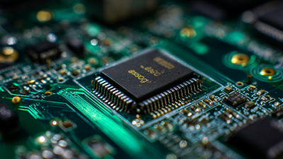
Selecting the right materials is crucial for enhancing the efficiency of printed circuit board (PCB) designs. The choice of substrate material can significantly impact the overall performance of the PCB. For instance, using high-frequency laminates like Rogers or PTFE can reduce signal loss at microwave frequencies, making them ideal for RF applications. Furthermore, considering thermal conductivity is essential; materials like aluminum-backed PCBs are excellent for applications requiring effective heat dissipation, thereby improving reliability and longevity.
In addition to substrate materials, the selection of conductive materials plays a vital role in ensuring efficient electrical performance. Copper is the most common choice due to its low resistivity and excellent thermal conductivity. However, for specialized applications, alternatives such as gold or silver may be used to enhance performance further, especially in high-frequency or high-reliability scenarios. Additionally, the integration of low-loss dielectrics can minimize signal degradation, allowing for higher data transfer rates and improved overall efficiency in electronic devices. By carefully selecting these materials, designers can significantly optimize the performance and efficiency of their PCB layouts.
Implementing Effective Layout Strategies for Reduced Signal Loss
When designing printed circuit boards (PCBs), reducing signal loss is paramount for enhancing overall efficiency. Effective layout strategies can significantly mitigate issues related to signal integrity. According to a report by the IPC (Institute of Printed Circuits), nearly 35% of electronic failures in modern circuits can be traced back to poor PCB layout and inadequate signal routing. Therefore, adopting a disciplined approach to layout is essential for optimizing performance.
One of the primary strategies is to minimize trace lengths and avoid unnecessary bends. Longer traces can introduce additional capacitance and inductance, which can distort the signal. A study by the IEEE (Institute of Electrical and Electronics Engineers) highlights that for every inch of trace, the signal integrity degrades by approximately 0.2 dB at high frequencies. Additionally, utilizing proper grounding techniques and incorporating ground planes can drastically reduce the likelihood of electromagnetic interference (EMI), which is crucial in high-speed applications. Implementing these strategies not only improves signal quality but also contributes to the overall reliability of the PCB design.
Utilizing Simulation Tools for Improved Design Accuracy
Utilizing simulation tools is critical in enhancing the accuracy of PCB electronics design. These advanced tools allow designers to visualize and test circuit behavior under various conditions before physical manufacturing takes place. By utilizing simulation software, engineers can identify potential issues, such as signal integrity problems or thermal management challenges, early in the design process. This proactive approach not only saves time and resources but also minimizes the risk of costly redesigns and production delays.
Moreover, simulation tools enable detailed analysis of electromagnetic interference (EMI) and power distribution networks, which are crucial for optimizing performance. Through iterative testing and modification, designers can fine-tune components and layouts to achieve greater efficiency. The ability to run multiple scenarios in virtual environments allows for informed decision-making and fosters innovative design solutions that traditional methods may overlook. Embracing these technologies is fundamental for any team looking to maximize the efficiency and reliability of their PCB designs.
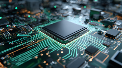
Incorporating Thermal Management in PCB Designs for Longevity
Effective thermal management is crucial in optimizing PCB designs for maximum efficiency and longevity. High temperatures can adversely affect the performance and reliability of electronic components. To combat this, designers should incorporate various strategies, such as careful component placement, heat sinks, and thermal vias. By placing heat-sensitive parts away from high-heat-generating components, the overall thermal profile of the PCB can be improved. Additionally, utilizing thermal vias can facilitate heat dissipation through the layers of the board, making it easier for heat to escape.
Another essential aspect of thermal management is the use of materials with good thermal conductivity. Selecting the right substrate materials can significantly influence heat distribution and overall efficiency. For instance, materials like copper-clad laminates offer better heat dissipation properties than standard FR-4 materials. Moreover, designing for airflow around the PCB can enhance cooling, especially in densely packed environments. Incorporating these thermal management techniques not only extends the lifespan of the components but also ensures the PCB operates within optimal temperature ranges, ultimately leading to improved system performance and reliability.
How to Optimize Your PCB Electronics Design for Maximum Efficiency - Incorporating Thermal Management in PCB Designs for Longevity
| Parameter |
Value |
Description |
| Max Operating Temperature |
85°C |
Maximum temperature for PCB components |
| Thermal Resistance |
10 °C/W |
Resistive heat dissipation of PCB |
| Preferred Material |
FR-4 |
Common dielectric material for PCBs |
| Copper Thickness |
1 oz/ft² |
Standard copper layer thickness |
| Cooling Solutions |
Heat Sinks, Vents |
Methods to dissipate heat efficiently |
| Design Rule Check (DRC) Compliance |
100% |
Ensures all thermal guidelines are followed |
| Heat Generation |
5 W |
Total heat produced by components |
| Thermal Simulation Tools |
ANSYS, SolidWorks |
Software used for thermal analysis |